Silicon Carbide Bonding Solutions
Advanced SiC Wafer Bonding Methods Successfully Address Critical Integration Challenges
Anonymous
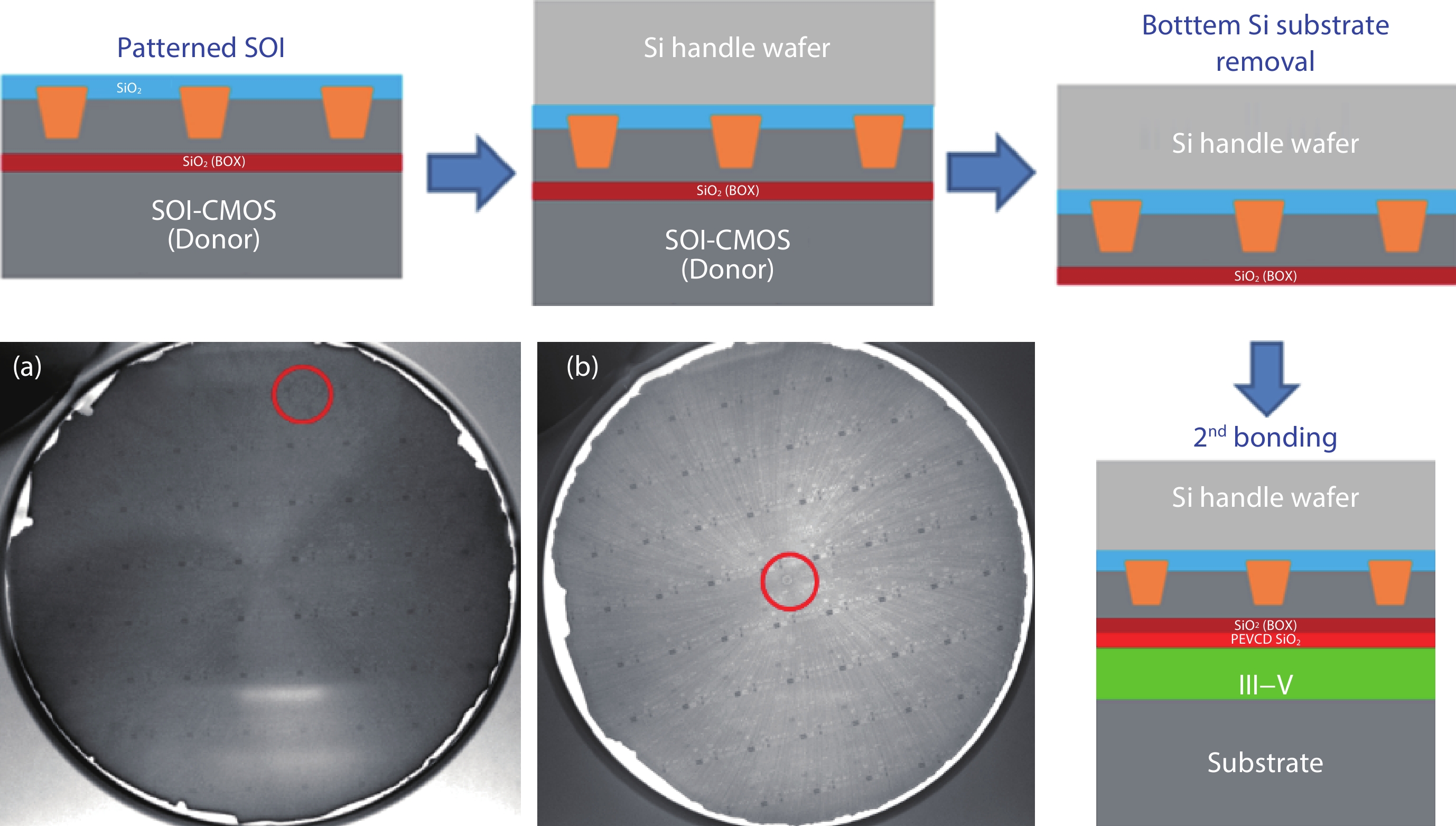
Silicon carbide wafer bonding enables device makers to combine SiC’s wide bandgap, high breakdown strength, thermal conductivity and chemical stability with separate layers that provide electrical conduction, heat spreading, mechanical support or optical access. Because SiC is chemically stable and mechanically hard, reliable bonding depends on controlling surface chemistry, atomic roughness, particles, trapped gases, stress and differences in thermal expansion. Direct bonding can produce a thin, clean and thermally efficient interface through surface forces and annealing, while indirect methods use metals, polymers, solders or other layers to ease processing and improve compatibility. However, intermediate layers may increase thermal resistance, electrical losses, contamination and long-term reliability risks, making the choice of bonding method dependent on performance, temperature, materials and production requirements.
Key Points
1
Direct SiC bonding may begin through van der Waals forces, hydrogen bonding or electrostatic attraction before pressure or annealing creates stronger surface bonds.
2
The bonding interface is itself part of the device architecture: its thickness, chemistry, defects, stress and thermal boundary resistance can determine whether a material stack performs successfully at wafer scale.
3
The articles note that Semicera’s technical department and researchers have conducted studies aimed at finding the best balance and outcome for SiC wafer bonding.
Sentiment
Mostly NegativeNEGATIVENEUTRALPOSITIVE
Publishers
5
Articles
11
Reach
16
A
AnonymousAuthor


