India Semiconductor Expansion
India invests ₹1.64 trillion to build a full domestic semiconductor manufacturing ecosystem.
Anonymous
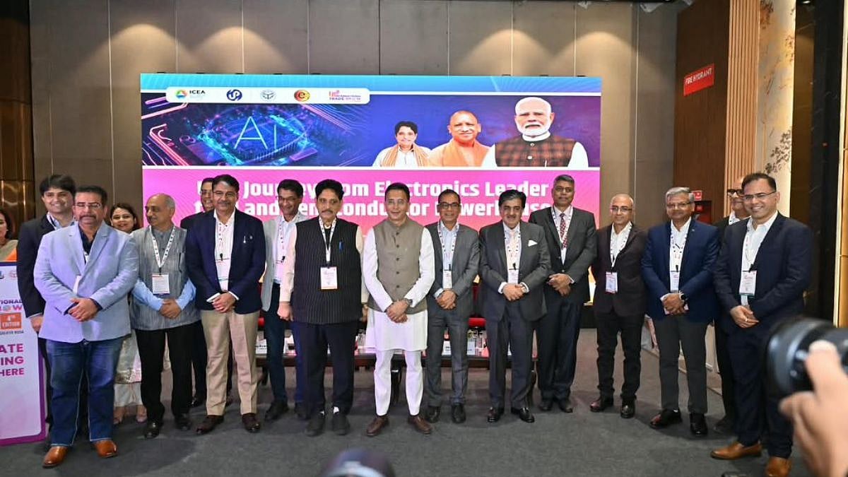
India is moving beyond its established strength in semiconductor design toward building a full domestic ecosystem spanning fabrication, assembly, packaging, materials, equipment, research and electronics manufacturing. The strategy is driven by rising demand from artificial intelligence, data centers, automobiles, communications and industrial automation, as well as supply-chain and national-security concerns. Government programs, including the India Semiconductor Mission, Production Linked Incentive schemes and Semicon 2.0, are supporting projects and attracting investment from global companies, while industry leaders are calling for closer coordination across manufacturers, suppliers, research institutions and end users. The opportunity extends beyond wafer fabrication to engineering, equipment, materials, advanced packaging and chip-design companies, allowing India to capture more value across the supply chain. Projects in Gujarat, Odisha and Uttar Pradesh indicate that the effort is progressing from policy to industrial implementation, but semiconductor plants require specialized infrastructure such as reliable power, high-purity water, cleanrooms, waste treatment and secure logistics. The expansion is therefore expected to reshape industrial corridors, employment centers and surrounding urban and real-estate markets as India seeks a larger role in global semiconductor supply chains.
Key Points
1
India accounts for more than 20% of the world’s semiconductor design workforce, and nearly every major fabless company has an active design centre in the country—providing an established talent base for the shift into manufacturing.
2
Semicon India 2026 drew more than 600 exhibitors, including nearly 300 international companies, and generated 56 MoUs, strategic initiatives and industry announcements spanning manufacturing, design, packaging, artificial intelligence, research, logistics and skilling.
3
Semicon 2.0 has an outlay of ₹1.275 trillion and covers six areas: semiconductor design; machines and materials; new fabrication plants; ATMP/OSAT packaging and testing; research and development; and talent. The government has received investment commitments of about ₹1 trillion under the programme, expected to materialise over the next two to three years.
4
Applied Materials has announced a $5 billion investment in India over the next decade, including spending on research, supply-chain development and talent, illustrating the role of global equipment companies in India’s semiconductor localisation effort.
5
Semiconductor manufacturing requires more than factory space: plants depend on cleanroom air filtration, high-purity water, specialised chemicals and gases, silicon wafers, precision equipment, high-capacity power infrastructure and logistics systems capable of safely handling sensitive materials.
Sentiment
Mostly PositiveNEGATIVENEUTRALPOSITIVE
Publishers
16
Articles
8
Reach
24
A
AnonymousAuthor


